When we think of ways to drive costs down for printed circuit boards (PCBs) today, it seems the first choice is to browbeat fabricators into submitting lower bids. That’s neither healthy nor right. Because they are your technology partners, you need them to be financially healthy.
If, instead, we look at material costs as a potential area for savings, we can find fertile ground for cost savings that an original equipment manufacturer (OEM) can control.
Many OEMs consider panelization a manufacturing task and blindly delegate those decisions to their suppliers, both fabrication and assembly. They are missing an opportunity to affect material
savings, one of the leading cost drivers for PCBs. Additionally, OEMs usually have multiple suppliers they work with: some for fabrication, others for assembly, and different ones for prototype versus production. Each supplier has their own panelization constraints and preferences.
Thus, the communication process between OEM and each of their suppliers is repeated and inefficient, and little is done to maximize material utilization consistently across all suppliers.
Ultimately, though, the OEM is responsible for their products’ costs.
ESTABLISHING CLEAR COMMUNICATION
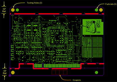
Between OEMs and suppliers, there can be confusion about what the term “panel” means. The assembly panel is the deliverable the OEM expects back from the fabricator (Figure 1). It is the product that will be put onto the assembly line. It does not necessarily imply multiple PCBs within the array, although it often times does. At a minimum, it includes the PCB, tooling holes, fiducials,
and frequently at least one rail for the SMT line to use for transporting.
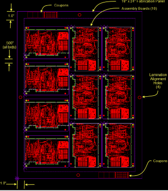
The fabrication panel (Figure 2) represents how the assembly panel will be configured while going through the fabrication process. It almost always entails a stepped and repeated image of the assembly panel onto a panel size the fabricators use. The fabrication panel will most certainly contain other features such as coupons, nomenclature, venting, and thieving patterns, as
well as their own tooling holes. While the fabrication panel configuration is ultimately the fabricator’s responsibility, knowing how the assembly panel will fit within a fabricator’s panel provides insight into the potential cost of the assembly panel.
OPPORTUNITIES TO REDUCE COSTS AND IMPROVE EFFICIENCY
There is also a tendency to dismiss the significance of material costs during prototyping because the number of panels needed is usually quite small. The objective is to get a small number of functioning boards to test. The costs that drive prototyping are affected mostly by the delivery timeframe required, whether the design has constrained nets, and the types of material and finish that are required. But often, once the prototypes are successful, the same PCB and the same assembly panel are assumed to be acceptable for production. However, acceptable and optimized are not the same.
Additionally, there are significant inefficiencies in the design-to-manufacturing (DFM) release process when it comes to panels. The typical flow is for the OEMs to use guidelines provided by their assembly supplier as input in drawing their assembly panel layout. These guidelines are documents that are interpreted by each person doing the assembly panel drawing and then created using an application different than the one used to design the PCB.
Finally, it is sent as a drawing file to the fabricator. The fabricator then interprets the drawing file and re-enters the configuration in their CAM system, generating a checkplot to be sent back to the OEM for validation before proceeding to tool for production. Only then does the OEM know how many panels are going to be
needed for the build and their costs. That’s a lot of wasted resources on something that’s not complicated.
Instead, an OEM should consider incorporating the assembly and fabrication suppliers’ panel guidelines into a software tool that removes the risk of interpretation and the redundancies of recreating each time. A real benefit is the early visibility the OEM has on cost effects of the material for the design and assembly panel. This facilitates consideration of alternative layouts of the assembly panel to lower the material costs.
With this early visibility, some high-volume OEMs will even want to evaluate changes to the PCB profile if it will give them greater material utilization in production. For example, a PCB designer for a mobile-communications OEM was able to increase material utilization from 52 to 88% by redefining a board feature that
allowed interlocking the PCBs in a panel—basically free money.
PREVENTING PROBLEMS RATHER THAN FIXING THEM LATER
For panelization software to fully benefit the process, it must be able to do all the tasks required. Otherwise, you do not have full visibility of the true cost-saving opportunities. Valor NPI’s Panel Optimization software:
•Stores the panel guidelines of all your fabrication and assembly partners.
•Quickly and easily creates panels optimized for both assembly and fabrication.
•Considers panel size, rail widths, margins, moat width, number of boards, and component overhang.
•Performs actions including pattern filling, addition of tooling holes, fiducials, bad board marks, targets, text, barcode, breaktabs, v-score lines, and rout.
•Creates and places breaktabs while automatically avoiding the placement of a breaktab under a component.
•Calculates exact material utilization to identify cost impact.
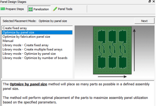
To aid in the panelization process, Valor NPI has added placement model selection assistance to the start of the process. The Panel Assistant (Figure 3) presents all available methods for designing panels. Upon the selection of the desired method, the specific required information will be presented and the panel design will be created. When determining the optimal assembly panel the ideal size is a function of the targeted fabrication panel size. This optimization solution will take a minimum and maximum number of arrays requested and the targeted panel size(s), then derive
and display all assembly panel design alternatives, ordered by material utilization.
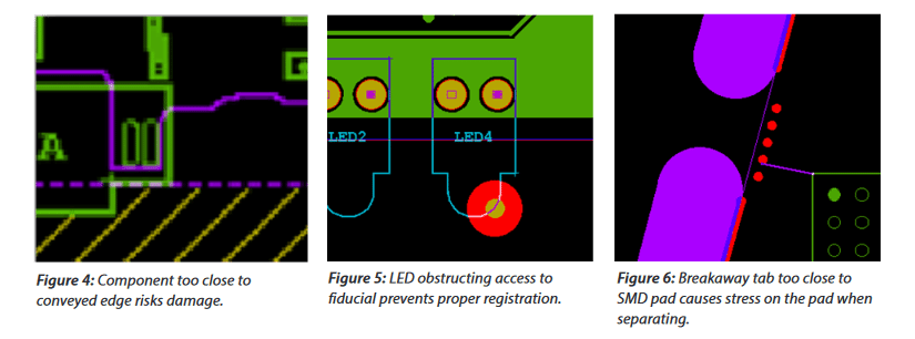
Another important consideration is what steps were taken to ensure the assembly panel configuration did not introduce its own manufacturing issues? Many issues in your assembly panel can be created without knowing it, only to have the fabricator report back that they cannot build it as designed. Even worse, some of these issues might not manifest until the assembly panels reach the assembly operation, making it a costly mistake. DFM software can be used to systematically check for assembly panel issues.
Figures 4–6 are some examples of manufacturing issues often introduced by the assembly panel.
A side benefit of taking control of panelization is that the OEM can view suppliers’ requirements and be assured the output sent to them is not only acceptable, but optimized, for the OEM’s objectives. This process will also save the inefficiencies of having to communicate and resolve the same topics with each supplier. This consistency is further enabled by sending the panel data as part of the ODB++ container provided them, instead of as a drawing file.
EXAMPLE OF SAVINGS ON MATERIALS
Let’s talk about material utilization percentages. Fabricators provide a number that is usually impressively high, say above 60%. It sounds good but is deceiving. The fabricator is stating how much of the fabrication panel is being used based on the assembly panel provided them. The assembly panel is always a rectangular box that fits into rectangular panels quite nicely.
www.mentor.com
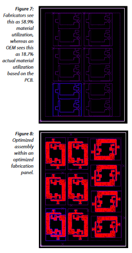
In reality, what the OEM cares about is the actual material area used for the PCBs, not the assembly panel, because that determines how many panels need to be built for the order. As illustrated in Figure 7, the fabricator will report this material utilization at 58.9%, but because of the shape of this PCB, the actual material utilization is only 18.7%.
At Mentor, we studied four different designs, each with their own definition of production volume, to measure the potential material savings to an OEM. PCB 1 is a rigid PCB built in lot sizes of up to 2,000. Figure 8 illustrates that before panel optimization, the OEM was getting 18.7% material utilization on an 18 x 24 in. fabrication panel with two PCBs per array and six arrays per panel.
When the OEM optimized their assembly panel, they found they could get 31.5% material utilization, yielding 10 arrays of 2 PCBs per fabrication panel. The Valor NPI panel design and optimization software automatically nested circuits into a tighter assembly panel in spite of its non-standard shape.
We then applied the results to a simple costing spreadsheet that considered:
• Number of PCBs ordered.
• Fabrication panel square area.
• Fabrication panel cost per square inch.
• Fabrication panel overage needed (to accommodate scrap).
The fabrication panel overage is a variable because lower percentages are required with higher volume. All other variables were considered to be constant between the two scenarios.
For the first example, we calculated the costs before and after panel optimization for order sizes between 100 and 2,000, in increments of 100.
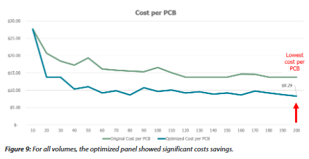
As shown in Figure 9, in all volumes the optimized panel showed significant costs savings. Furthermore, we identified the order size that yielded the lowest cost per PCB. Which begs the question, would you change your order size if you knew where the lowest possible cost per PCB is?
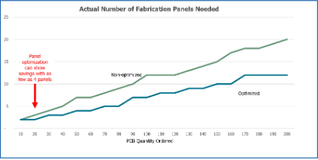
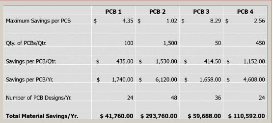
Figure 10 shows the actual number of fabrication panels needed, non-optimized and optimized. While it might initially be surprising that these lines are not entirely straight, they reflect the combination of variables previously stated. What may be even more surprising is that panel optimization can show cost savings in as few as four panels for this design.Lastly, over a test sample of four PCBs, again each with their own production volume, there are impressive savings across the board, even when only a small number of PCBs are designed
each year (Table 1).
Lastly, over a test sample of four PCBs, again each with their own production volume, there are impressive savings across the board, even when only a small number of PCBs are designed each year
(Table 1).
As an added bonus, when considering the labor costs involved to define, create, and communicate all the panelization instructions, a systematic panelization tool also can have meaningful labor savings.
SUMMARY
OEMs are ultimately responsible for the cost of their products, including the PCBs. While every fabricator will certainly optimize the fabrication panel based on the constraints of the assembly panel they receive, the OEM often does not know the cost implications of their PCB or assembly array until it is too late. By taking responsibility for the panel design and optimization process during the PCB design process, and the visibility that provides, the OEM stands to reap significant material costs savings and accelerate their time to market.
Remember, you might think you are buying PCBs, but you are paying for panels. The fewer you need, the lower your costs.