
This blog is the last blog in a three part series on the topic of shunt resistor connections where the second blog discussed making accurate connections and the first discussed diagnosing errors.
Today, we are going to look at the shunt resistor connection of a PCB design and compare measurement accuracy data between a PCB with a good connection and a PCB with a bad connection.
When making a shunt connection use recommended connections to the shunt resistor. The connection traces should be of equal length, equal dimension and as short as possible. Be sure to ensure the current sense amplifier and the shunt resistor are on the same side of the PCB. For the highest level of accuracy use four terminal shunts also know as Kelvin shunts.
In Figure 1 below, the green box surrounds the area of the sense line traces from the shunt resistor to the input pins. The traces leading to the resistor pad are of equal length, dimension and they terminate at the center of the inside of the pad relative to where the shunt resistor connects to the pad.
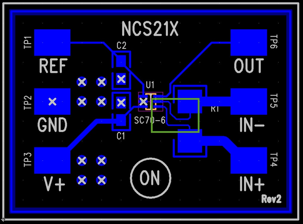
Figure 1: NCS21xR Customer Evaluation PCB Layout with Optimized Connections to Shunt Resistor
Figure 2 shows the two customer evaluation boards used for this current shunt measurement experiment. The board on the left, labeled “Good” has a 1 mΩ shunt soldered neatly across the resistor pads (R1) and the sense line connections are optimized based on typical manufacturer recommendations on how to connect to a two terminal shunt.
The board on the right, labeled “Bad” is configured exactly the same as the “Good” board, with the exception of the connection of the sense traces to the shunt. To illustrate the undesirable effects of an incorrect shunt connection, the sense lines were simply cut and rerouted to a different location on the sense resistor pads to emulate an incorrectly designed PCB board connection.